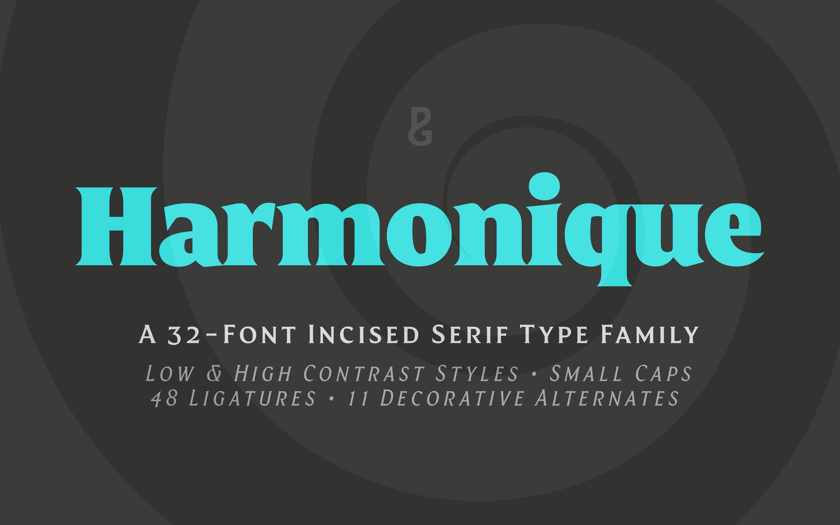
An Incised Serif Type Family

This typeface is part of The Monotype Library.
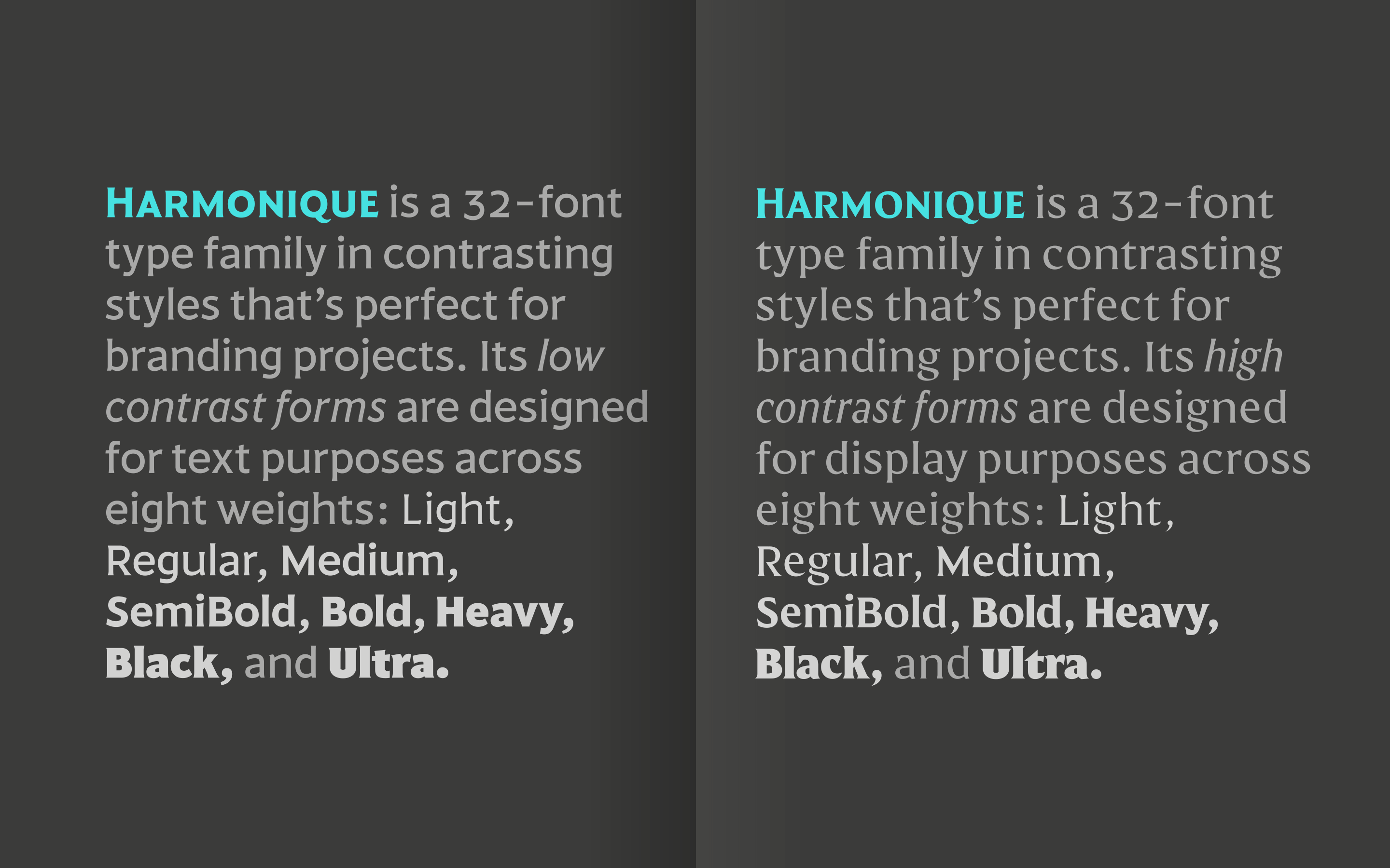
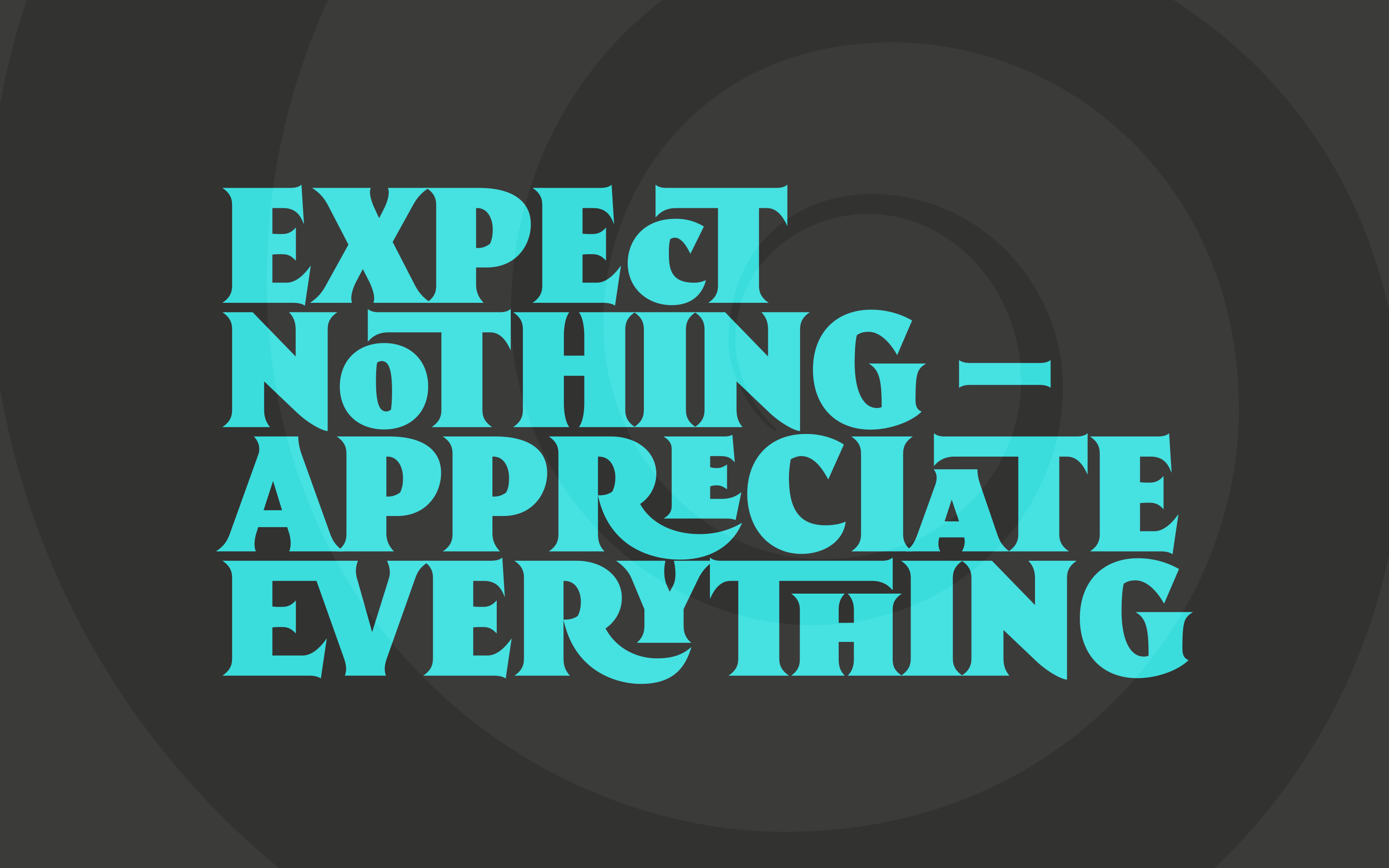
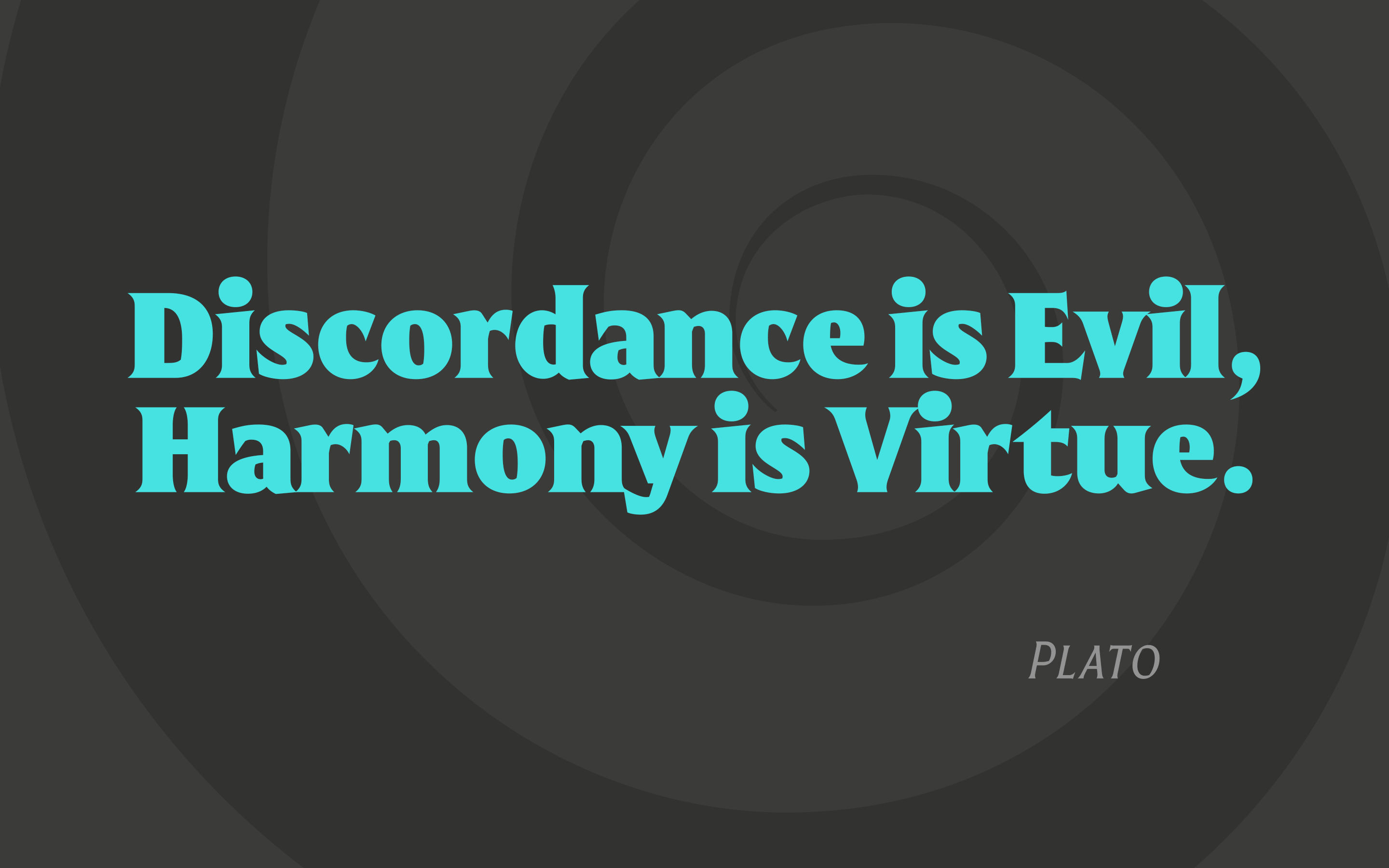
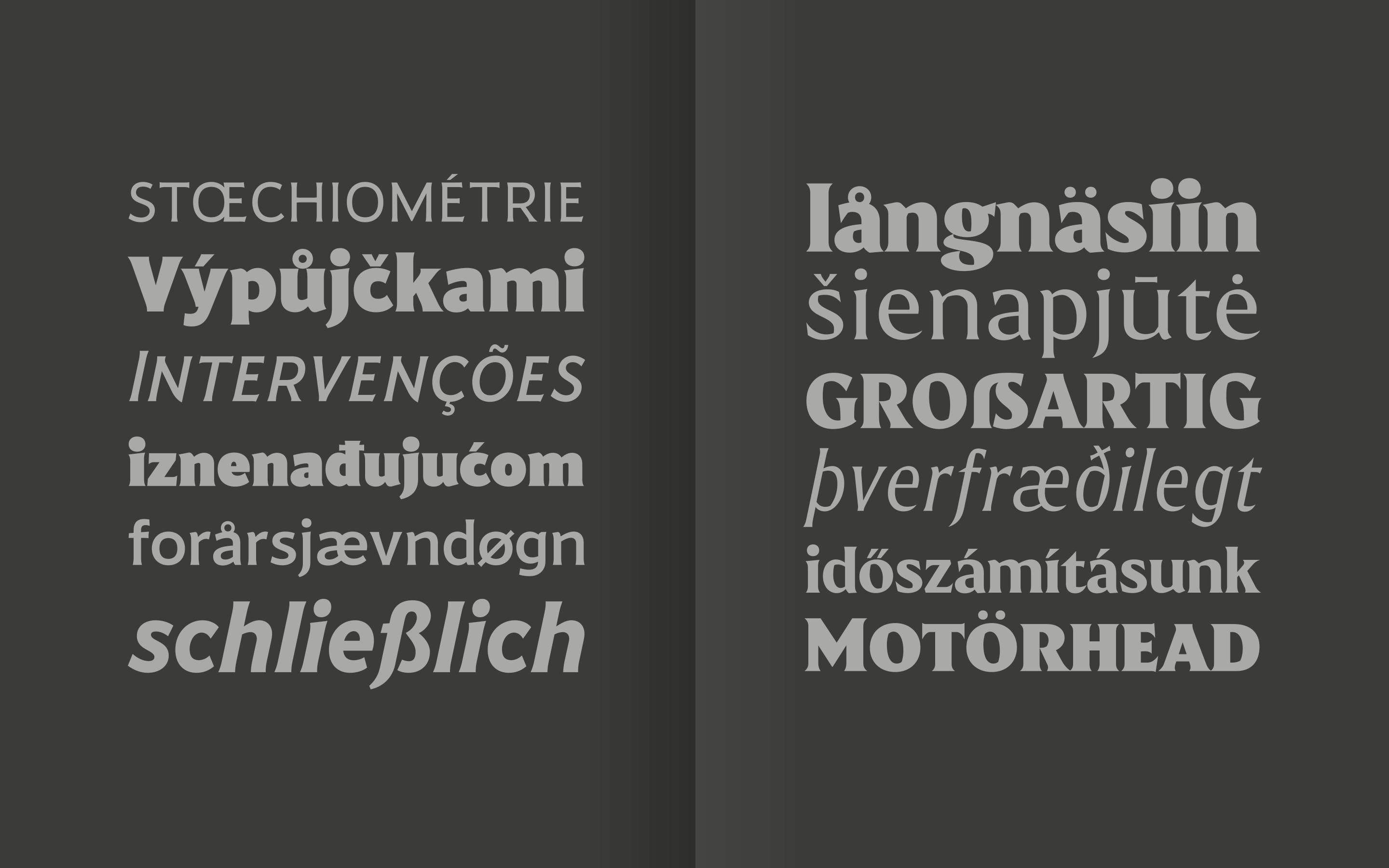
Harmonique is an incised serif typeface designed for both text and display purposes. It’s a type family of two styles that work in harmony together to add distinction and personality to your own typographic compositions. Harmonique’s low contrast forms have the appeal of a humanist sans serif typeface. Its subtly flared terminals evoke the craft and skill of a signwriter’s steady hand, creating an authentic and pleasing aesthetic. Harmonique Display is more calligraphic in its structure – as if drawn by a wide-nibbed pen. This style is accentuated by aggressively barbed serifs and chiselled arcs in its counters and bowls. These strong characteristics help to define a flamboyant, confident style that will provide impact and flair to your headlines, titles and identity designs.
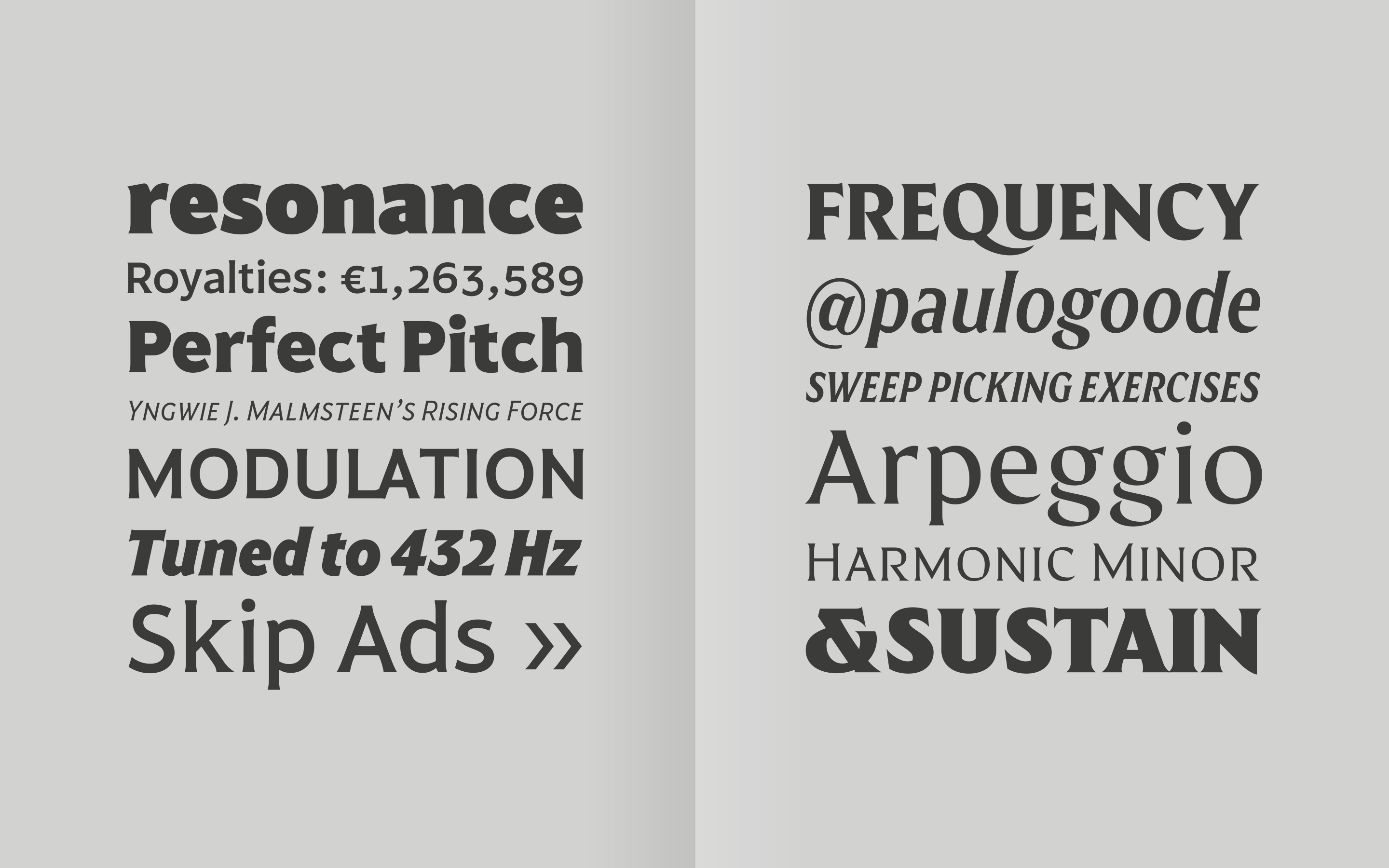
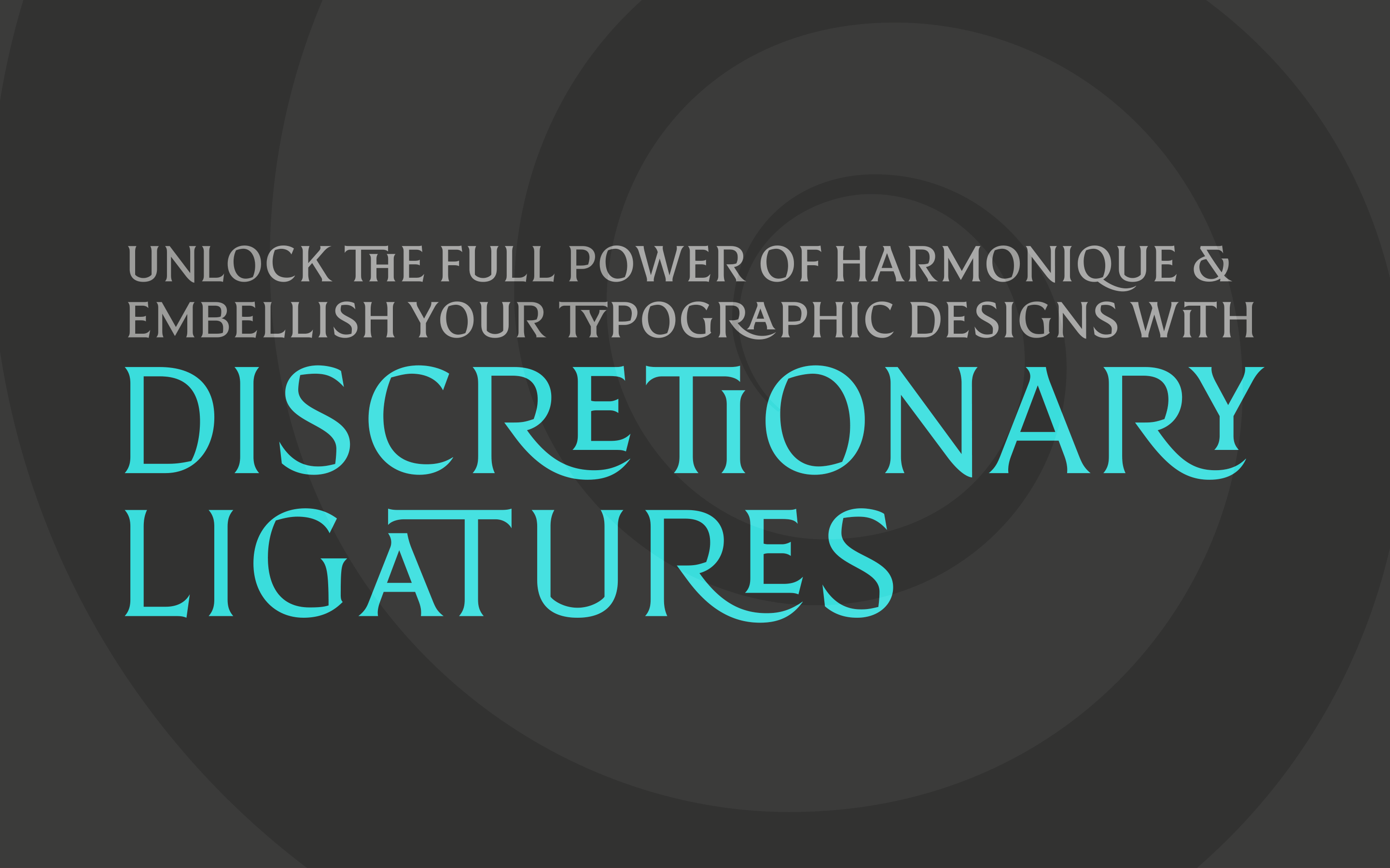
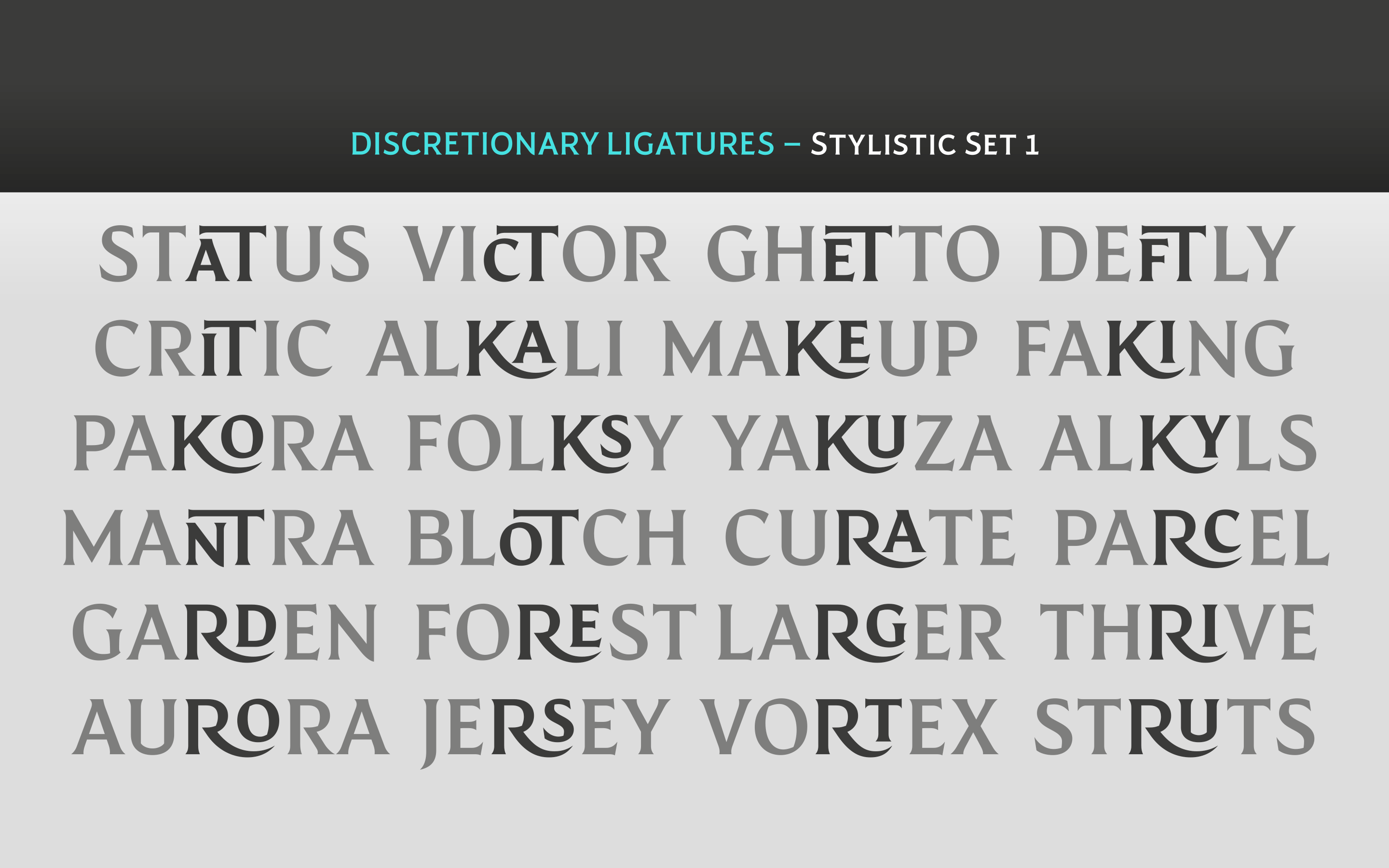
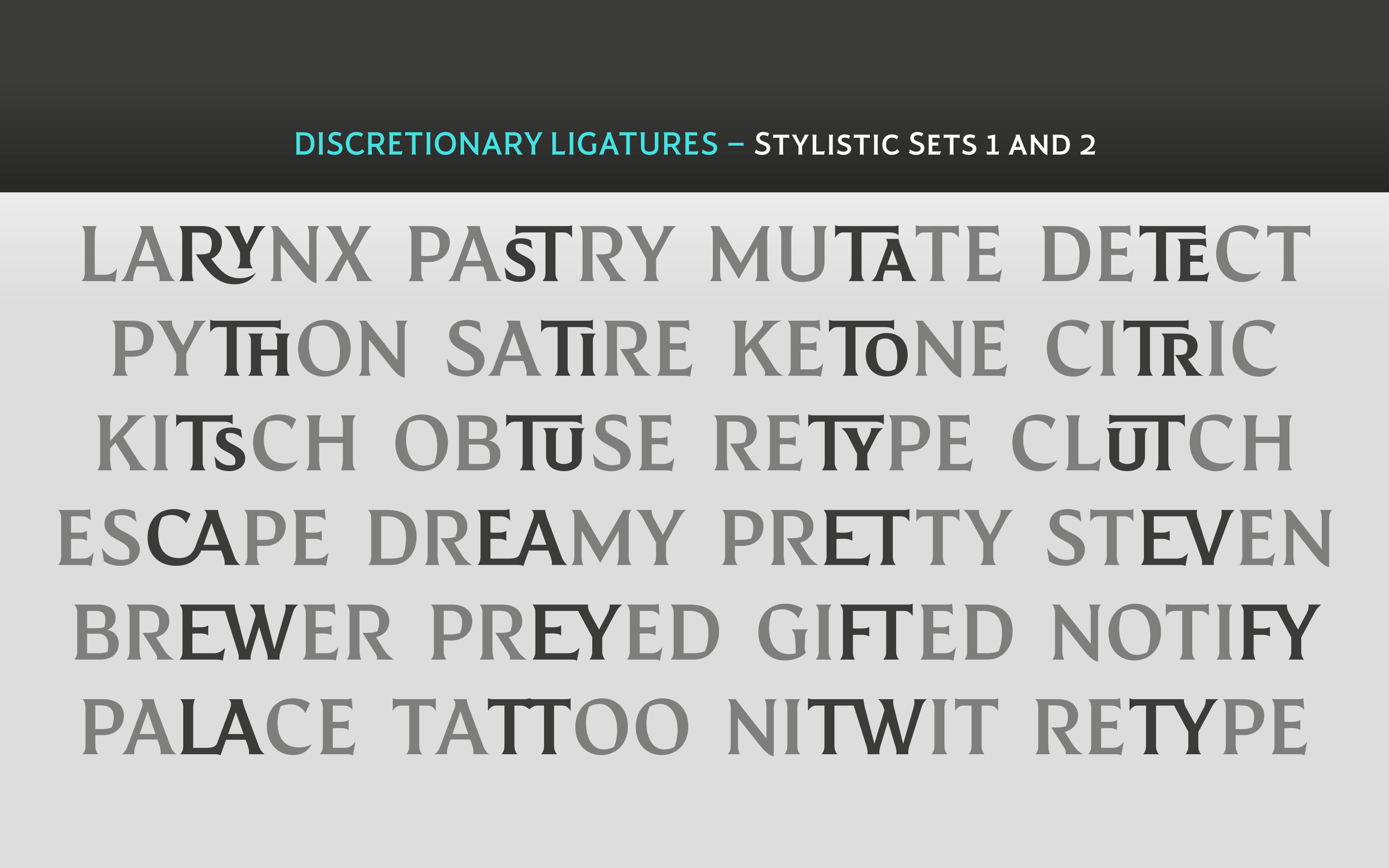
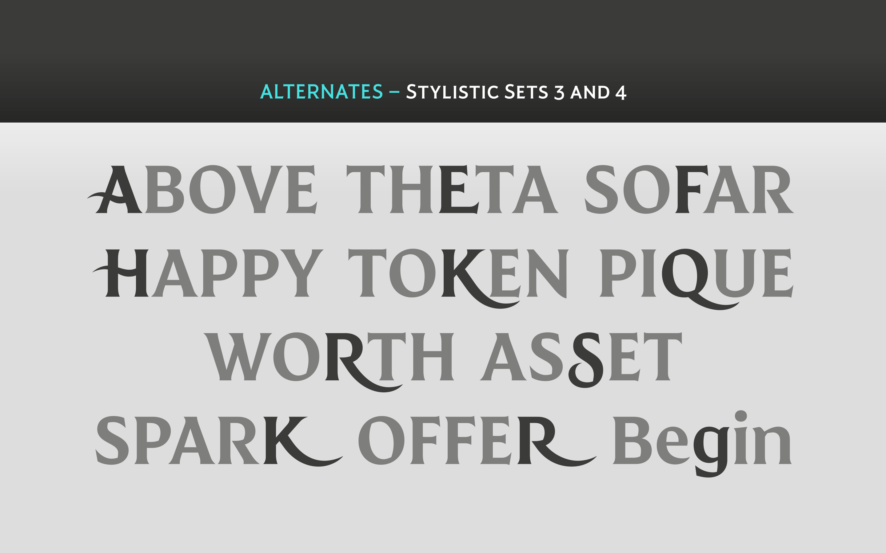
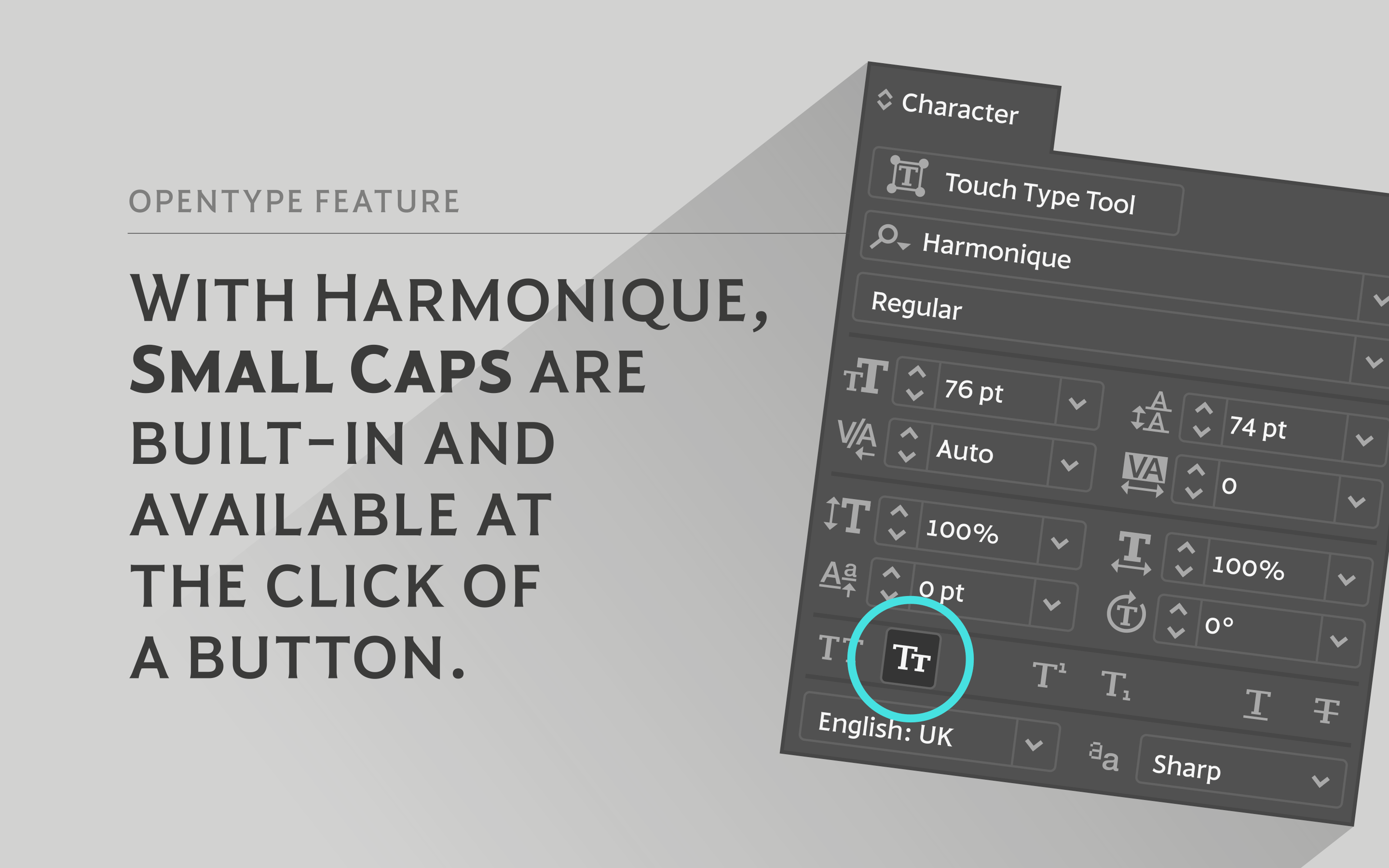
Practical features include 48 ligatures that will enhance titling possibilities with their all-capital pairings – these are accesssed by turning on Discretionary Ligatures and then selecting either Sylistic Set 1 or 2. There are also a number of alternate caps that will subtly enhance your titles and headlines – access these via Stylistc Sets 3 and 4. Small Caps are included too (along with their matching diacritics) – adding another layer of versatility to this typeface. Proportional Lining figures are available as an option if you prefer them to the default Old Style figures.
There are 32 fonts altogether, with 8 weights in roman and italic from Light to Ultra in both text (low contrast) and display (high contrast) styles. Harmonique has an extensive character set (650+ glyphs) that covers every Latin European language.
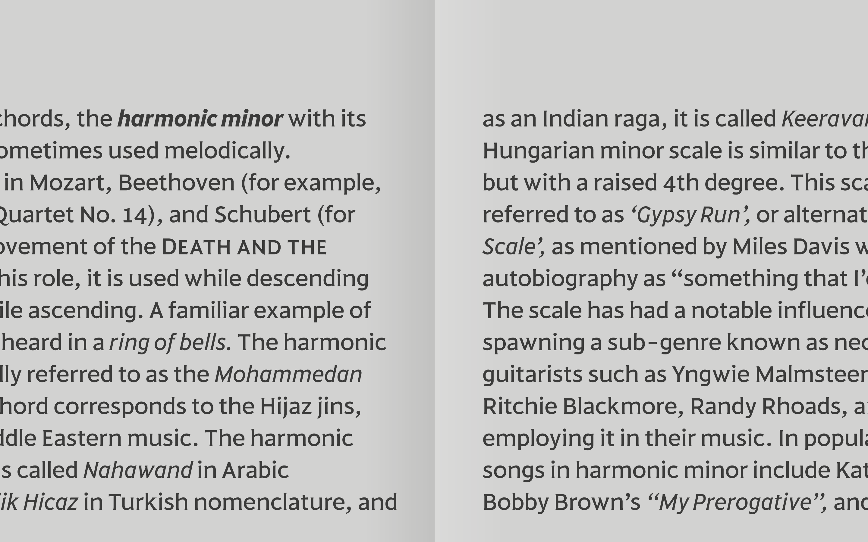
SUGGESTED FONT PAIRING: Harmonique and Stasis.
| Release Date | April 2021 |
| Classification | Incised Serif |
| No. of Fonts | 32 |
| Weights & Styles |
|
| Alternates | 11 |
| Ligatures | 48 |
| Small Caps | Yes |
| No. of Glyphs | 650+ |
| Language Support | European – Latin Only |
Locate the physical Samsung KMGD eMMC chip on the board. The test point is usually a tiny, gold-plated circular pad situated immediately adjacent to the edge of the chip package.
A precision screwdriver set, plastic opening picks, anti-static tweezers (or a conductive copper wire), and a high-quality USB data cable.
Note: The plastic housing can discolor near 280°C, but electrical integrity remains intact under 260°C.
Once your layout is complete and approved for manufacturing, lock the X and Y coordinates of your KMGD test points in your EDA software (such as Altium Designer, KiCad, or Allegro). Changing their positions later will render expensive custom test fixtures completely useless. Conclusion kmgd test point
: BGA-221 layout, commonly found in budget-to-mid-range smartphones, IoT gateways, and embedded devices manufactured between 2017 and 2022.
There were limits. Test points can perturb the thing they measure: probe capacitance can dampen fast edges; shunt resistances can load delicate nodes. KMGD’s design balanced accessibility with non-invasiveness — high-impedance buffering, judicious placement, and clear labeling so technicians would use the right adapters. The engineering team documented best practices: always use a grounded tip, avoid long alligator leads for high-speed sampling, and consider active probes for gigahertz domains.
Push the probe firmly into the test point until you hear a slight click. The internal valve opens, and system pressure is routed to your gauge. Ensure the gauge’s range exceeds the system’s maximum possible pressure. Locate the physical Samsung KMGD eMMC chip on the board
: As devices get smaller, test points might need to become smaller and more precisely located, possibly leading to new techniques for accessing and utilizing them.
| Challenge | Consequence | Mitigation | |-----------|-------------|-------------| | Pad lifting due to repeated probing | Board failure | Use PTH test points (ring+plated barrel); limit re-probe cycles to < 20 | | Oxidized pad → poor contact | False test failures | Specify ENIG finish; store boards in low-humidity environment | | Inadequate spacing | Probe shorting during ICT | Follow 1.27 mm minimum pitch; use staggered placement for dense designs | | Missing ground reference | Noisy measurements | Add dedicated G points every 50 mm on large boards | | Test point on flexible PCB | Pad peel-off | Reinforce with stiffener or use small surface-mount test pins (e.g., Keystone 5000 series) |
A hardware test point (often abbreviated as TP) is a small, exposed copper pad or pin on a device’s printed circuit board (PCB). Factory Diagnostics Note: The plastic housing can discolor near 280°C,
A test point is a deliberate instrumentation location inserted into kernel code (driver, kernel module, or OS core) to:
In the world of hardware repair and data recovery, certain cryptic labels on a circuit board can mean the difference between a successful fix and a permanent "brick." One such label often encountered by technicians working on legacy hardware or specialized industrial boards is the KMGD test point
A powerful diagnostic tool for advanced users and technicians, though it carries high risks for those without hardware experience. Core Features